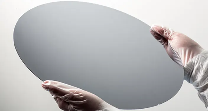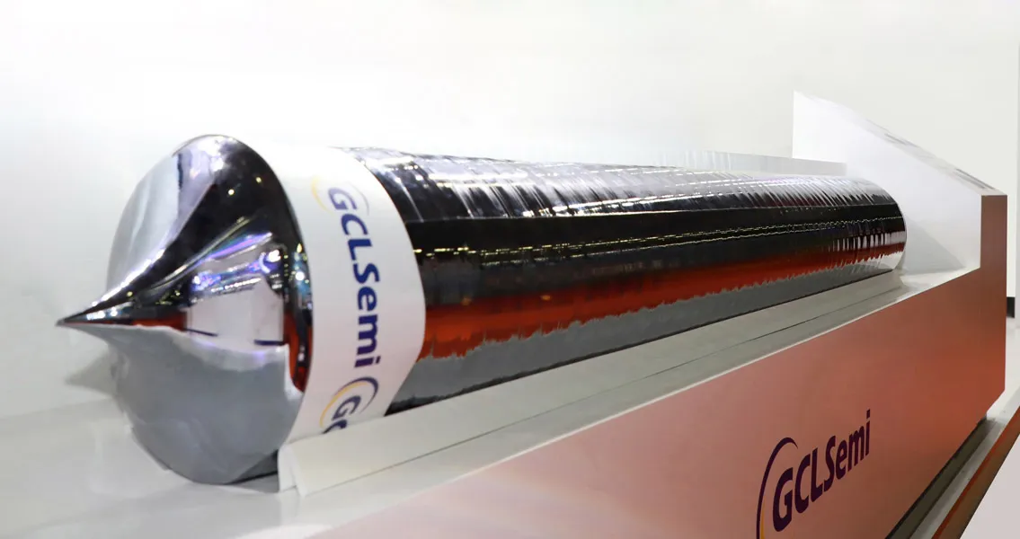
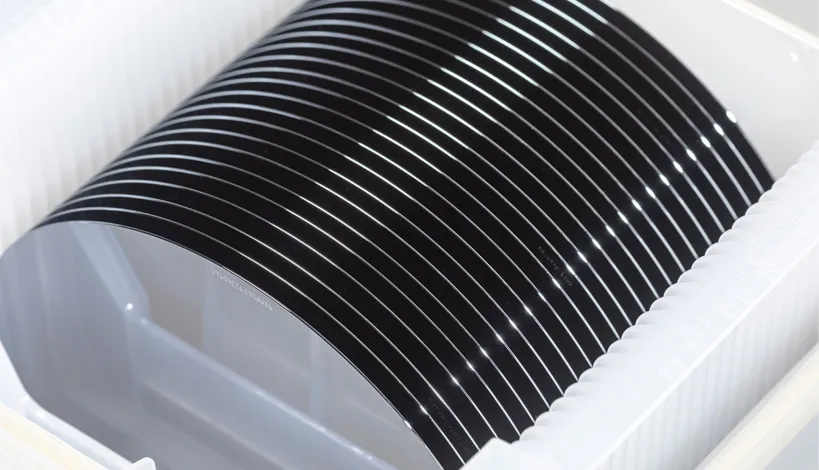
GCLSemi is located in Xuzhou Economic and Technological Development Zone, Jiangsu Province, with a registered capital of 4.21 billion yuan and a planned manufacturing capacity of 600,000 pieces / per month, is a high-technology enterprise dedicated to the research and development and manufacturing of 300mm semiconductor silicon wafers. The company had started production in October 2020, with a complete range of products, including polished wafers, epitaxial wafers, customized silicon wafers, silicon rods and other specifications.
The company has a team of skillful international talents plus a sizeable and practical fab facility. In 2021, the company's products had been applicable for 28-nanometer chip manufacturing in batches, and had achieved breakthrough 14-nanometer technology node verification, and we have made gradual advancement to 10-7nm advanced process. The company has an advanced crystal laboratory, a USA based R&D Center and a Xuzhou Research & Development Institute (Semiconductor materials), including a full set of design and production capabilities of independent research and development of key patented-crystal pullers, heat field, software and hardware system.
Through independent research and development and technology integration, the company has invented and applied more than 500 types of patented technologies, which GCLSemi has the most comprehensive patent setup in the local China's silicon wafer industry. The company has obtained ISO9001, ISO14001, ISO45001, IATF16949 system certification, our products have passed the qualification of mainstream integrated circuit customers in China mainland, China Taiwan, Japan, United States of America and Singapore.
 Focus on us