On August 18, 2022,The company was listed and mentioned as the " Top 10 most promising companies, within the new industry standard in 2021-2022 China’s Integrated Circuit and Semiconductor Industry Listing.

On March 23, 2022 The company had held it's first year 2022 shareholders' meeting.
In February 2022, the company completed a series A financing of 1.64 billion yuan.

On January 24, 2022, the company had passed the IATF16949:2016 Quality Management System Certification of SGS and obtained the IATF16949:2016 compliance certificate.

In December 2021, the company completed the Equity Incentive Proposal for middle-level and senior executive partners.

In December 24, 2021, We had been shortlisted as " Jiangsu Province Semiconductor Company's -Large silicon wafer cutting and polishing Workshop – in the “Model of Intelligent Manufacturing Demonstration Workshop Listing.”

In the fourth quarter of 2021, the company has successfully produced a 12-inch epitaxial wafer that meets the specifications of 14nm wafer manufacturing standard, and the product entered into the mainstream of customer verification stage.

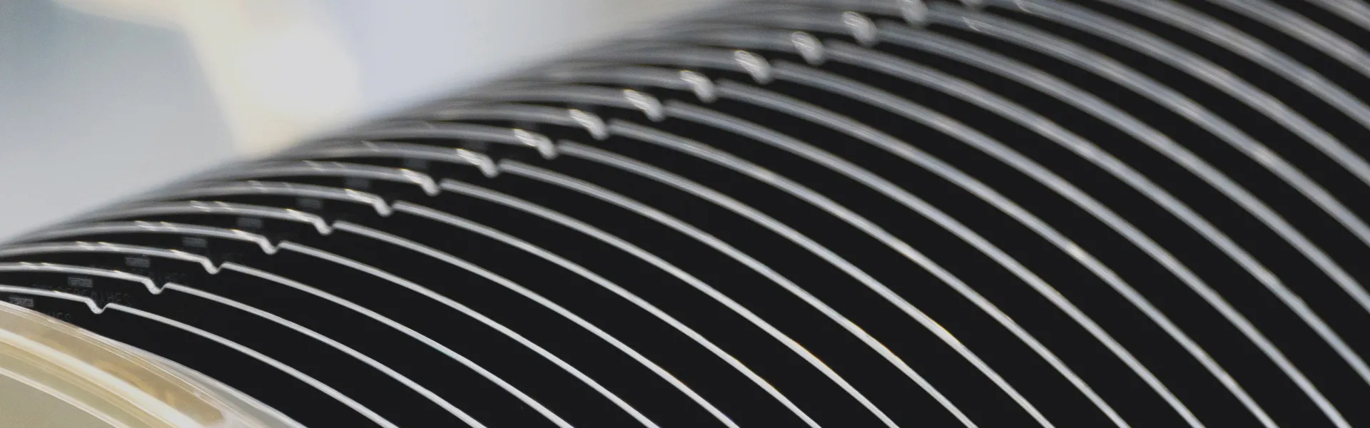
Third Quater of 2021, the company had successfully achieved the company's 12-inch silicon wafer products' certification for our core customers from China Taiwan, United States of America , Japan.. and signed many permanent sale orders.

In August 2021, the perfect crystal yield of our Rui-O 300 Crystal puller has reached the international level standard.

On June 23, 2021, GCLSemi and China University of Mining and Technology jointly held the "Off-campus Internship Base" award ceremony.

December 9, 2020, GCLSemi obtained SGS ISO9001:2015 quality system certification.

On October 9, 2020, the first batch of 300mm/28nm large silicon wafer products started mass production line in GCLSemi.

In January 2020, the semiconductor large silicon wafer project of GCLSemi was approved and recognized by the relevant state ministries and commissioning authority.

On October 14, 2019, the first 12-inch semiconductor-grade silicon ingot was pulled in advanced crystal Laboratory of GCLSemi forming one perfect crystals.

In December 2018, the semiconductor large silicon wafer project of GCLSemi was supported by Provincial Strategic Emerging Industry Special Funds in Jiangsu Province.

In August 2018, GCLSemi semiconductor large silicon wafer project had officially started ground-breaking ceremony.

 Focus on us